Memory Wall Emerges as the Biggest Challenge of the AI Era

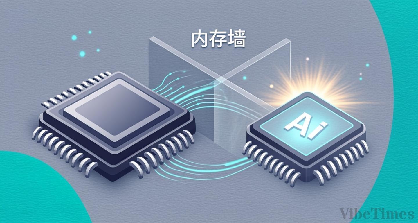
Samsung Electronics has set out to overcome the 'Memory Wall,' the biggest challenge of the AI era. The Memory Wall refers to a problem caused by the gap in data supply speeds between processors and memory as AI models grow larger, and it determines how fast AI responds. The problem is especially pronounced during the decoding stage, where AI generates its answers, since the speed of reading trained data and temporary storage data determines response time. To solve this, Samsung Electronics has begun developing 'zHBM,' a next-generation memory that stacks processors and memory together in a single package.
High Bandwidth Memory (HBM) has established itself as the solution to this challenge. It vertically stacks multiple DRAM dies and connects them with through-silicon vias (TSVs) to exchange large volumes of data in parallel. Unlike conventional graphics-oriented GDDR memory, which relied on per-pin data transfer rates and hit limits in power consumption and heat, HBM has dramatically improved storage density and power efficiency. Across successive HBM generations, Samsung Electronics has increased the number of stacked dies to 12 and 16 while steadily expanding bandwidth and capacity.
At Samsung Electronics' booth at 'Semiconductor Expo (SEDEX) 2026,' held on the 14th at COEX in Gangnam, Seoul, the seventh-generation HBM 'HBM4E' was on display. HBM4E offers more than 20% faster processing speeds than HBM4, which began shipping this year. zHBM, introduced by Samsung Newsroom on the 28th, directly vertically stacks memory with processors such as GPUs or AI-specific ASICs, dramatically widening data pathways, while optimizing thermal management at the system level to maximize efficiency within limited power budgets. At the event, Samsung Electronics also showcased a zHBM mockup and 'zNAND-O,' a 3D NAND solution optimized for edge AI.
In the foundry segment, the company unveiled a base die built on a 4-nanometer process along with ultra-dense packaging technology, while in advanced packaging it exhibited '2.3D Cube-E,' which uses silicon bridges, and '3D Cube-H,' which vertically stacks chips.